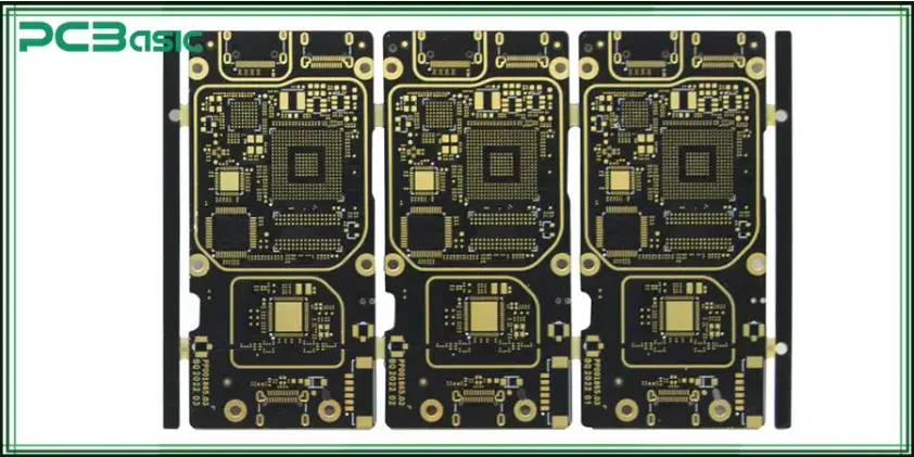
As modern electronics continue to push performance boundaries, high frequency PCBs and advanced component packaging, such as Land Grid Arrays (LGAs), are becoming increasingly common. LGAs are widely used in high-speed processors, FPGAs, and RF modules due to their compact size, high pin count, and excellent electrical performance. However, combining high-frequency signals with LGA packages poses unique challenges in PCB design—particularly in signal integrity, layout optimization, and thermal management.
This article explores key considerations when designing high frequency PCBs for LGA components to ensure optimal performance and reliability.
1. Understanding the Characteristics of LGA Packages
LGA (Land Grid Array) packages connect to the PCB via flat contact pads rather than leads or pins. Unlike BGA (Ball Grid Array), LGAs do not use solder balls; instead, they rely on solder paste applied directly to PCB pads, making them ideal for thin-profile, high-density applications.
Key advantages:
- Low inductance and resistance paths
- High interconnection density
- Minimal vertical height
- Strong mechanical stability
However, these benefits also introduce tight design tolerances, complex soldering profiles, and increased sensitivity to PCB warping or signal noise—especially in high-frequency environments.
- Signal Integrity in High Frequency PCB Design
In high-frequency applications (typically above 500 MHz), signal degradation can significantly impact performance. LGAs, with their short and compact connections, help reduce some parasitics—but only if the PCB layout supports proper signal propagation.
Key Signal Integrity Considerations:
- Impedance Matching:
Maintain controlled impedance for high-speed traces using microstrip or stripline structures. Use field solvers or impedance calculators to model trace geometry accurately. - Short and Direct Traces:
Minimize trace length between LGA pads and nearby components to reduce signal reflection and propagation delay. - Differential Pair Routing:
For interfaces like USB, PCIe, or LVDS, ensure differential traces are length-matched and tightly coupled with consistent spacing. - Ground Plane Strategy:
Place a continuous ground plane under high-speed traces and LGA pads to reduce return path discontinuity and crosstalk. - Via Minimization:
Avoid excessive use of vias in high-frequency paths as they can introduce signal reflections and stubs. Use back-drilling or blind/buried vias where necessary.
2. PCB Layout Strategies for LGA and High-Frequency Signals
Layout is critical when combining LGA packaging with high-speed signals. Proper pad design, layer stacking, and signal routing all impact final performance and manufacturability.
Recommended Practices:
- Pad Design & Solder Mask:
Use non-solder-mask-defined (NSMD) pads for LGA footprints to ensure better solder joint reliability. Maintain consistent solder paste volume to avoid tombstoning or open connections. - Via-In-Pad Design:
Avoid placing vias directly in LGA pads unless filled and capped properly; otherwise, solder wicking can lead to poor connections. - Component Placement:
Place high-speed ICs and critical components as close as possible to the LGA to minimize trace lengths and parasitic effects. - Power Distribution:
Use solid copper planes and multiple vias for power and ground connections to ensure low impedance paths. - Layer Stackup:
Design a symmetric stackup with dedicated high-speed routing layers sandwiched between reference planes for signal shielding and impedance control.
3. Thermal Management Challenges
High-speed components in LGA packages often generate considerable heat. Since LGAs lack leads that assist with heat dissipation, thermal design must be handled primarily at the PCB level.
Thermal Design Techniques:
- Thermal Vias:
Incorporate a matrix of thermal vias beneath the LGA to conduct heat from the component into internal ground/power planes or to a heatsink. - Copper Plane Integration:
Add large copper pours under and around the LGA area for heat spreading. - Heatsinks & Thermal Pads:
Use thermal interface materials (TIMs) and heatsinks where component specifications require direct heat extraction. - Simulation & Testing:
Conduct thermal simulation during the design phase to validate heat dissipation paths and monitor hotspots during prototype testing.
Manufacturing and Assembly Considerations
LGA soldering requires tight control over reflow profiles and paste deposition due to its flat contact interface. Warping, uneven solder volume, or insufficient heating can lead to open or weak joints.
- Stencil Design: Use laser-cut stencils with carefully tuned aperture sizes to maintain consistent paste height.
- Reflow Profile: Ensure a stable thermal gradient during reflow to prevent component movement or cold joints.
- Inspection: Employ X-ray inspection and electrical test methods to confirm connection integrity post-assembly.
Conclusion
Designing high frequency PCBs for LGA packages demands precision and expertise across multiple domains—electrical, thermal, and mechanical. By addressing signal integrity, optimizing layout strategies, and managing thermal challenges, engineers can fully unlock the performance advantages of LGA-based systems. Whether you’re designing RF modules, embedded processors, or next-gen communication systems, incorporating these best practices ensures high-speed reliability and manufacturability in your final product.
Also Read-Should I start collecting video games?


